1.4.2.1. LED Counter
Note
The instructions here are an example for STEMlab 125-14. For other boards, different flags must be used. The design source structure may differ from the one seen in the pictures here. Please see the Vivado Project Setup for more information.
1.4.2.1.1. Prepare the environment
Download and extract the Red Pitaya FPGA Git repository to a folder/directory on your computer.
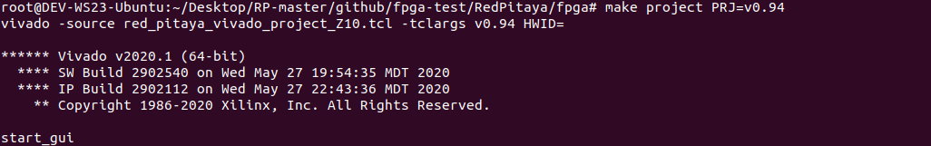
Open Vivado, and in “Vivado Tcl Console”, navigate to the base folder RedPitaya-FPGA and make a clean Red Pitaya Vivado project.
. /opt/Xilinx/Vivado/2020.1/settings64.sh
cd Downloads/
cd RedPitaya-FPGA/
make project PRJ=v0.94 MODEL=Z10
On Windows, search for Vivado HLS 2020.1 Command Prompt and launch it.
Using the command line, navigate to the extracted folder and make a Vivado project:
cd Downloads/
cd RedPitaya-FPGA/
make project PRJ=v0.94 MODEL=Z10
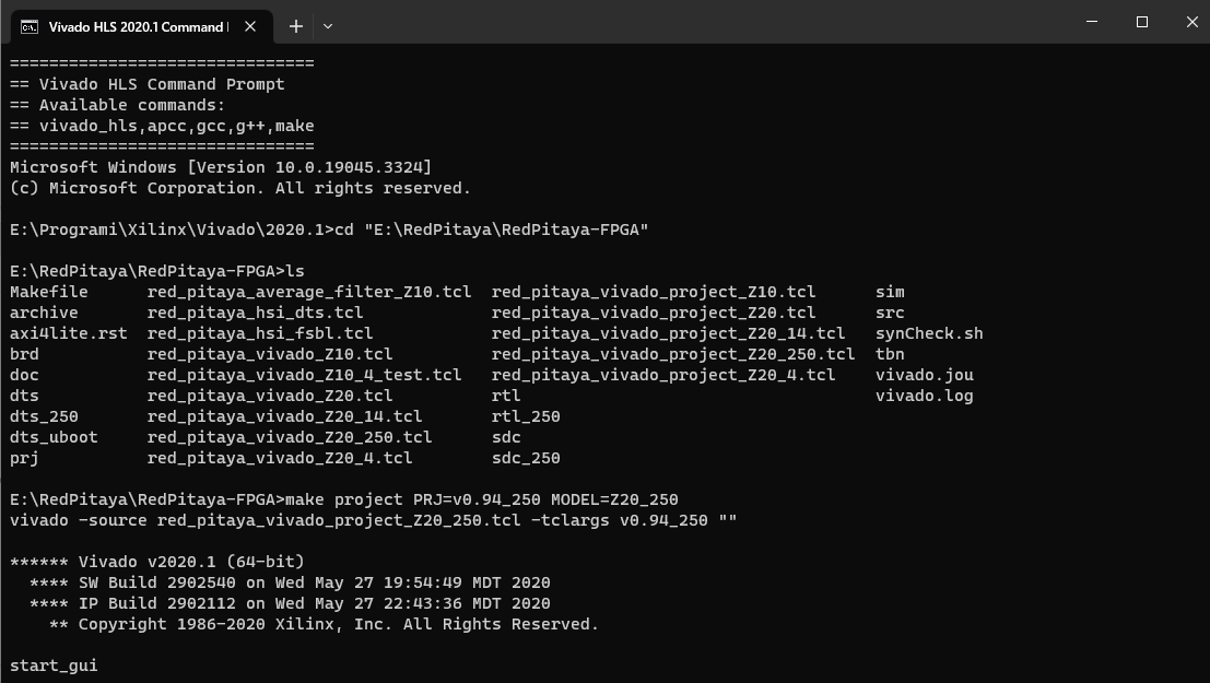
This will automatically generate a complete project in the RedPitaya-FPGA/prj/v0.94 directory.
1.4.2.1.2. Description
In this project, we will learn how to create a simple LED binary counter using basic VHDL code. We will also learn how to replace one of the rarely used components in the Red Pitaya FPGA, the MIMO PID, and replace it with our own FPGA component. This way, the system bus can easily be used to give programs access to registers and, with a few minor modifications, gain access to ADCs and DACs, but let us not get ahead of ourselves.
Our FPGA component will contain the code for a binary LED counter, but later on, you can use the same structure and completely reprogram the functionality.
Most of the FPGA code for Red Pitaya is written either in Verilog or in System Verilog. We can even include a component written in VHDL to the project without problems.
In the Sources window, under Design Sources, are all the HDL (Hardware Description Language) files included in our project. These can be either written in VHDL or Verilog. If you look closely, you will see that one of the files is highlighted in bold and has a small green-grey pyramid in front of the name. This file is called the “Top” module. It contains all other modules and FPGA code that is included in our project. In our case, the Top file is named red_pitaya_top.sv. If we expand the drop-down menu of the red_pitaya_top, we can see all the modules that are included in the project. All other modules that are not located under the red_pitaya_top are still in our overall FPGA project, but they will not affect the overall functionality (we could say that they are commented out).
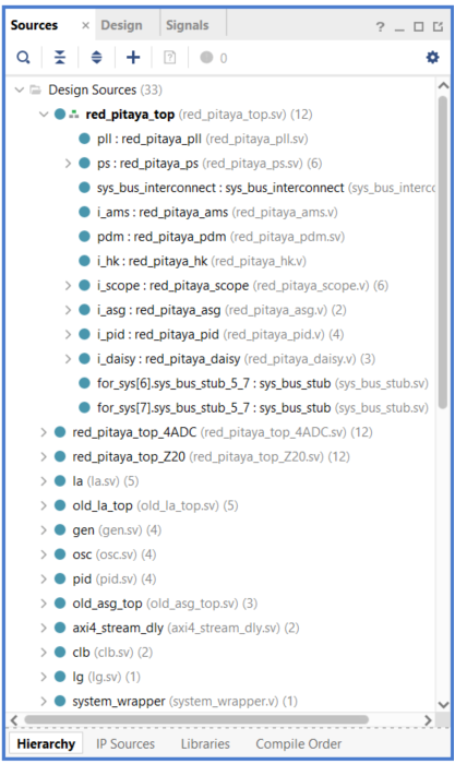
If you look closely, you will notice that some of the modules included under the top module red_pitaya_top can also be expanded. This means that they also contain multiple submodules. Each module contains Verilog or VHDL code and can include other HDL files/modules as components. A similar example is including a library in our C or Python program.
We can think of each module as a black box with inputs and outputs that perform a specific task. We can connect this black box to other black boxes like LEGOs so that together they can perform a more complex task. Multiple smaller boxes can fit inside a larger one. Each box can also contain smaller ones. Let’s say we are building a LEGO car. Once our LEGO car has been built, it represents the biggest black box or the topmost module of the FPGA program. But the LEGO car is not just one single LEGO brick; We had to build it from scratch with the general idea in mind. Our LEGO car is composed of multiple parts: Doors, seats, engine, chassis, and other components. Each of these represents a sub-module, all connected to form a fully functioning car. Each of the sub-modules (the engine, for example) may also be composed of sub-modules. The smallest of them may contain only a few LEGO bricks (lines of code) that together perform the specified task.
Enough of the theory; let’s dive in.
1.4.2.1.2.1. Red_Pitaya_top.sv
We can see that our red_pitaya_top has twelve other submodules (pll, ps, sys_bus_interconnect, etc.). One of them is named “i_pid”. We will replace it with our own component named i_led.
Double-click on the red_pitaya_top to open the file inside Vivado’s code editor. In the comments at the top (lines 10-40), we can see how the modules are connected together, then there is the definition of all input and output signals of the red_pitaya_top component. The one we are interested in is the LED signal in line 110.
Since we want to “blink” the LEDs, we need to change the port logic to output:
// LED
output  logic [ 8-1:0]
Scrolling downwards, we can see the definitions of local signals and parameters, and finnaly component connections. Since it will take a while to find how the LEDs are connected let us use Ctrl+F and type in “led” to find where and how the signal is connected.
In line 425 we spot the following code:
red_pitaya_hk i_hk (
  // system signals
  .clk_i           (adc_clk ),  // clock
  .rstn_i          (adc_rstn),  // reset - active low
  // LED
  .led_o           (  led_o                      ),  // LED output
  // global configuration
  .digital_loop    (digital_loop),
  .daisy_mode_o    (daisy_mode),
  // Expansion connector
  .exp_p_dat_i     (exp_p_in ),  // input data
  .exp_p_dat_o     (exp_p_out),  // output data
  .exp_p_dir_o     (exp_p_dir),  // 1-output enable
  .exp_n_dat_i     (exp_n_in ),
  .exp_n_dat_o     (exp_n_out),
  .exp_n_dir_o     (exp_n_dir),
  .diag_i          (locked_pll_cnt_r2),
   // System bus
  .sys_addr        (sys[0].addr ),
  .sys_wdata       (sys[0].wdata),
  .sys_wen         (sys[0].wen  ),
  .sys_ren         (sys[0].ren  ),
  .sys_rdata       (sys[0].rdata),
  .sys_err         (sys[0].err  ),
  .sys_ack         (sys[0].ack  )
);
As we can see, the led_o port is connected to a housekeeping section. Disconnect it.
// LED
//.led_o           (  led_o                      ),  // LED output
In lines 447-450 we see the comment for the LED section, but it is currently empty. Here is where we will include our own LED module as a component. The next thing we need to find is the PID component and disconect it. It is located on lines 528-550. Our LED component will be connected in almost identical way, so we should copy the code and then comment out the “MIMI PID controller”:
///////////////////////////////////////////////////////////////////////////////
//  MIMO PID controller
////////////////////////////////////////////////////////////////////////////////

//red_pitaya_pid i_pid (
//   // signals
//  .clk_i           (adc_clk   ),  // clock
//  .rstn_i          (adc_rstn  ),  // reset - active low
//  .dat_a_i         (adc_dat[0]),  // in 1
//  .dat_b_i         (adc_dat[1]),  // in 2
//  .dat_a_o         (pid_dat[0]),  // out 1
//  .dat_b_o         (pid_dat[1]),  // out 2
//  // System bus
//  .sys_addr        (sys[3].addr ),
//  .sys_wdata       (sys[3].wdata),
//  .sys_wen         (sys[3].wen  ),
//  .sys_ren         (sys[3].ren  ),
//  .sys_rdata       (sys[3].rdata),
//  .sys_err         (sys[3].err  ),
//  .sys_ack         (sys[3].ack  )
//);
Note
On SIGNALlab 250-12, the MIMO PID is already commented. Instead, the followign lines need to be commented:
//assign sys[3].ack = 1'b1 ;
//assign sys[3].err = 1'b0 ;
//assign sys[3].rdata = 32'h0 ;
We should also make sure that the “pid_dat” signals are not left floating:
assign pid_dat[0] = 14'b0;
assign pid_dat[1] = 14'b0;
Now it is time to prepare the connection for our LED component. Scroll back to the LED section of red_pitaya_top and input the following code:
////////////////////////////////////////////////////////////////////////////////
// LED
////////////////////////////////////////////////////////////////////////////////

led i_led (
   // signals
  .clk_i           (adc_clk   ),  // clock
  .rstn_i          (adc_rstn  ),  // reset - active low
  .led_o           (led_o     ),    // LEDs
  //.dat_a_i         (adc_dat[0]),  // in 1
  //.dat_b_i         (adc_dat[1]),  // in 2
  //.dat_a_o         (pid_dat[0]),  // out 1
  //.dat_b_o         (pid_dat[1]),  // out 2
  // System bus
  .sys_addr        (sys[3].addr ),
  .sys_wdata       (sys[3].wdata),
  .sys_wen         (sys[3].wen  ),
  .sys_ren         (sys[3].ren  ),
  .sys_rdata       (sys[3].rdata),
  .sys_err         (sys[3].err  ),
  .sys_ack         (sys[3].ack  )
);
We have just connected a component called led that we named i_led. We comented out the ADC and DAC ports, which we will not be using in this example, connected the LEDs, and left everything else as is. This means we will be able to access the change the LEDs and access the System bus.
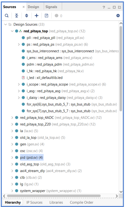
After we save the red_pitaya_top file, we can see that the PID component is now outside the red_pitaya_top and there is an unknown i_led file in its place, which we are going to create now.
1.4.2.1.2.2. led.vhd
Create a new design source file (click on the blue + in the Sources menu) ==> Add or create design sources ==> Create File. Name the new file led.vhd and select VHDL as the file type.
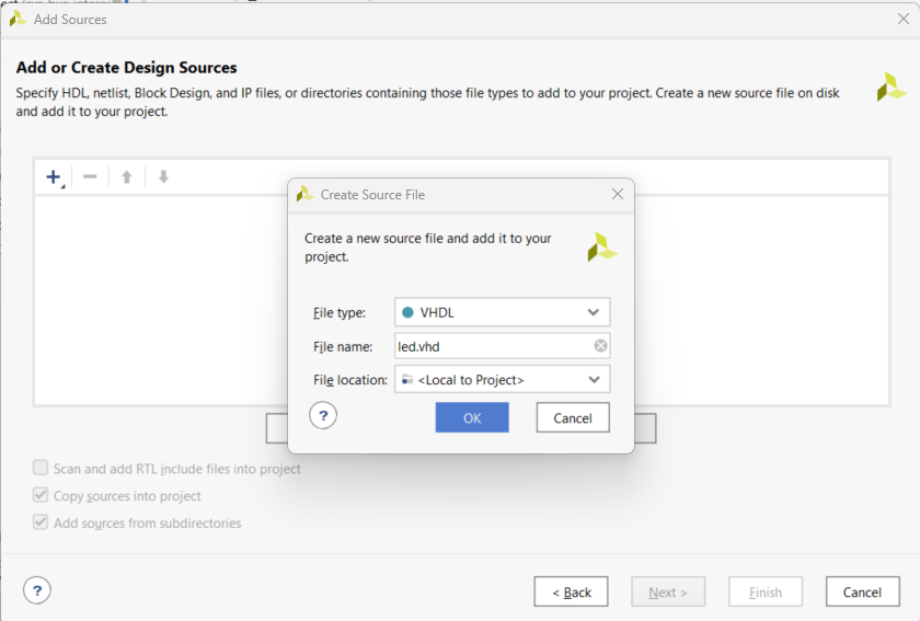
Click OK and skip the Define Module step. Confirm that the Module has not changed ==> OK. We will add all the ports manualy.
You should see that the undefined led component now has a file associated to it.
Open the i_led: led(Behavioral)(led.vhd) file and copy the following code into it, and save the file:
--------------------------------------------------------------------------------
-- Company: Red Pitaya
-- Engineer: Miha Gjura
--
-- Design Name: led
-- Project Name: Red Pitaya V0.94
-- Target Device: Red Pitaya STEMlab 125-14
-- Tool versions: Vivado 2020.1
-- Description: Led Counter code
-- Sys Registers: 403_00000 to 403_fffff (uses MIMO PID register space)
--------------------------------------------------------------------------------

library IEEE;
use IEEE.STD_LOGIC_1164.all;
use IEEE.NUMERIC_STD.all;

entity led is
  port (
    clk_i   : in  std_logic;                        -- bus clock
    rstn_i  : in  std_logic;                        -- bus reset - active low
    led_o   : out std_logic_vector(7 downto 0);     -- led bus
    sys_addr  : in  std_logic_vector(31 downto 0);  -- bus address
    sys_wdata : in  std_logic_vector(31 downto 0);  -- bus write data
    sys_wen   : in  std_logic;                      -- bus write enable
    sys_ren   : in  std_logic;                      -- bus read enable
    sys_rdata : out std_logic_vector(31 downto 0);  -- bus read data
    sys_err   : out std_logic;                      -- bus error indicator
    sys_ack   : out std_logic                       -- bus acknowledge signal
    );
end led;

architecture Behavioral of led is
    signal count_speed : unsigned(31 downto 0) := to_unsigned(1, 32);
    signal led_count : unsigned(31 downto 0) := (others => '0');

begin

    count: process(clk_i)
    begin
        if rising_edge(clk_i) then
            if rstn_i = '0' then
                led_count <= (others => '0');
            else
                led_count <= led_count + count_speed;
            end if;
        end if;
    end process;

    led_o <= std_logic_vector(led_count(31 downto 24));

    -- Handling non-connected system signals
    -- sys_ack <= '1';
    sys_err <= '0';

    --  Registers, write & control logic
    pbus: process(clk_i)
    begin
        if rising_edge(clk_i) then
            if rstn_i = '0' then

            else
                sys_ack <= sys_wen or sys_ren;    -- acknowledge transactions

--                if sys_wen='1' then               -- decode address & write registers
--                    if sys_addr(19 downto 0)=X"00054" then
--
--                    end if;
--                end if;
            end if;
        end if;
    end process;

    -- decode address & read data
    with sys_addr(19 downto 0) select
        sys_rdata <= X"FEEDBACC" when x"00050",   -- ID
                     X"00000000" when others;

end Behavioral;
So, what exactly does the code above do?
The entity contains all the signals that go in and out of our led module. These signals enable us to control the LEDs and access the System bus.
entity led is
  port (
    clk_i   : in  std_logic;                        -- bus clock
    rstn_i  : in  std_logic;                        -- bus reset - active low
    led_o   : out std_logic_vector(7 downto 0);     -- led bus
    sys_addr  : in  std_logic_vector(31 downto 0);  -- bus address
    sys_wdata : in  std_logic_vector(31 downto 0);  -- bus write data
    sys_wen   : in  std_logic;                      -- bus write enable
    sys_ren   : in  std_logic;                      -- bus read enable
    sys_rdata : out std_logic_vector(31 downto 0);  -- bus read data
    sys_err   : out std_logic;                      -- bus error indicator
    sys_ack   : out std_logic                       -- bus acknowledge signal
    );
end led;
In the architecture, we defined two signals. led_count contains the value of the counter with initial value of 0 and count_speed how fast the counter changes (set to 1).
architecture Behavioral of led is
    signal count_speed : unsigned(31 downto 0) := to_unsigned(1, 32);
    signal led_count : unsigned(31 downto 0) := (others => '0');

begin
In the count process, on each rising edge of the clock signal the led_count is increased by count_speed. And the upper eight bits are assigned to the led_o port.
count: process(clk_i)
begin
    if rising_edge(clk_i) then
        if rstn_i = '0' then
            led_count <= (others => '0');
        else
            led_count <= led_count + count_speed;
        end if;
    end if;
end process;

led_o <= std_logic_vector(led_count(31 downto 24));
Next, we have connected the sys_err signal that we are not using to 0.
-- Handling non-connected system signals
-- sys_ack <= '1';
sys_err <= '0';
This section is not used for this project, but it is an example of how you can change a value of a variable inside the FPGA (write data to FPGA), by writing a value to a specific registry address. Since this module is connected to the PID registry space, we can only use addresses between 403_00000 and 403_fffff, which is why we are only interested in the lower 20 bits of the system address bus.
--  Registers, write & control logic
        pbus: process(clk_i)
        begin
            if rising_edge(clk_i) then
                if rstn_i = '0' then

                else
                    sys_ack <= sys_wen or sys_ren;    -- acknowledge transactions

    --                if sys_wen='1' then               -- decode address & write registers
    --                    if sys_addr(19 downto 0)=X"00054" then
    --
    --                    end if;
    --                end if;
                end if;
            end if;
        end process;
Finaly an example of how to read data from the FPGA. In our case, we implemented a ID into the registry space. We can check whether our FPGA image is loaded, by reading from address 0x40300050, where we should get the value FEEDBACC in return.
-- decode address & read data
with sys_addr(19 downto 0) select
    sys_rdata <= X"FEEDBACC" when x"00050",   -- ID
                 X"00000000" when others;
1.4.2.1.2.3. Generate Bitstream and program the FPGA
We are ready to click on the Generate Bitstream button. After successful completion of synthesis, implementation, and bitstream generation, the bit file can be found at RedPitaya-FPGAprjv0.94projectredpitaya.runsimpl_1red_pitaya_top.bit.
How the FPGA is reprogrammed depends on the Red Pitaya OS version.
Please make sure that the PATH environment variable is set correctly. See Vivado installation guide for more information.
Note
On Windows, the process can also be done through a standard Command Prompt, but any echo commands must be executed inside the Windows Subsystem for Linux (WSL) Terminal (The output file encoding is a problem with Windows echo). For more information, refer to the following forum topics:
Please note that you need to change the forward slashes to backward slashes on Windows.
Open Terminal or CMD and go to the .bit file location.
cd <Path/to/RedPitaya/repository>/prj/v0.94/project/repitaya.runs/impl_1
Send the newly generated .bit file to the RedPitaya’s /root folder using WinSCP or type the following commands in the Linux console or Windows Command Prompt.
scp red_pitaya_top.bit root@rp-xxxxxx.local:/root/Led_counter.bit
Now establish an SSH communication with your Red Pitaya and check if you have the copy red_pitaya_top.bit in the root directory.
ssh root@rp-xxxxxx.local
redpitaya> ls
Finally, we are ready to program the FPGA with our own bitstream file located in the /root/ folder on Red Pitaya. To program the FPGA simply execute the following line in the Linux console your Red Pitaya:
redpitaya> cat Led_counter.bit > /dev/xdevcfg
The 2.00 OS uses a new mechanism of loading the FPGA. The process will depend on whether you are using Linux or Windows as the echo command functinality differs bewteen the two.
Please note that you need to change the forward slashes to backward slashes on Windows.
On Windows, open Vivado HSL Command Prompt and go to the .bit file location.
On Linux, open the Terminal and go to the .bit file location.
cd <Path/to/RedPitaya/repository>/prj/v0.94/project/repitaya.runs/impl_1
Create .bif file (for example, red_pitaya_top.bif) and use it to generate a binary bitstream file (red_pitaya_top.bit.bin)
Windows (Vivado HSL Command Prompt):
echo all:{ red_pitaya_top.bit } >  red_pitaya_top.bif
bootgen -image red_pitaya_top.bif -arch zynq -process_bitstream bin -o red_pitaya_top.bit.bin -w
Linux and Windows (WSL + Normal CMD):
echo -n "all:{ red_pitaya_top.bit }" >  red_pitaya_top.bif
bootgen -image red_pitaya_top.bif -arch zynq -process_bitstream bin -o red_pitaya_top.bit.bin -w
Send the newly generated .bit.bin file to the RedPitaya’s /root folder using WinSCP or type the following commands in the Linux console or Windows Command Prompt.
scp red_pitaya_top.bit.bin root@rp-xxxxxx.local:/root/Led_counter.bit
Now establish an SSH communication with your Red Pitaya and check if you have the copy red_pitaya_top.bit.bin in the root directory.
ssh root@rp-xxxxxx.localredpitaya> lsFinally, we are ready to program the FPGA with our own bitstream file located in the /root/ folder on Red Pitaya. To program the FPGA simply execute the following line in the Linux console your Red Pitaya:
redpitaya> /opt/redpitaya/bin/fpgautil -b Led_counter.bit.bin
Now, you should see the LEDs blink in the pattern of a binary counter. Congratulations on making it this far!!! Don’t worry, you did not destroy your Red Pitaya.
1.4.2.1.2.4. Reverting to original FPGA image
If you want to roll back to the official Red Pitaya FPGA program, run the following command:
redpitaya> cat /opt/redpitaya/fpga/fpga_0.94.bit > /dev/xdevcfg
redpitaya> overlay.sh v0.94
or simply restart your Red Pitaya.
1.4.2.1.3. Conclusion
In this section we have learned how to create a simple LED counter project in the Red Pitaya’s FPGA. We also found out that it does not matter if a specific module/component is written in Verilog or VHDL, because of the “black box” principle that HDL languages use. This project can easily be expanded to include the ADC and DAC, but that is a topic for another time.
1.4.2.1.4. Author & Source
Author: Miha Gjura.
Based on Red Pitaya FPGA code and University of Ljubljana Faculty of Electrotechics LNIV.
This teaching material was created by Red Pitaya.