1.4.2.3. Knight Rider
1.4.2.3.1. Introduction
A blinking LED is one thing, but a true light show is something one can be proud of. In the LED blink example, we built a very simple FPGA program that made one LED on the Red Pitaya blink. For such a simple project, we constructed the necessary logic by graphically connecting different blocks in Vivado’s IP Integrator without writing a single line of code. Of course, not all applications will be so simple and we will eventually have to learn hardware definition language (HDL). To get acquainted with Verilog HDL, we will in this project build an FPGA program for Red Pitaya where eight lights slide like in the cult series, The Knight Rider.
1.4.2.3.2. Verilog Module
To make Red Pitaya simulate the Knight Rider light sequence, we will use the Verilog language to write a custom module that will provide the logic behind the continuous light sequence. There are two popular hardware description languages: VHDL and Verilog. We will choose the latter since most of the official Red Pitaya FPGA code is written in Verilog and because it is somewhat similar to the C programming language, which some readers might be familiar with. Once the knight_rider module is written, we will test it and then incorporate it into the block design we created in LED blink example. We will also demonstrate how to use the parallel nature of an FPGA to create a double Knight Rider light sequence.
To start, open or create LED blinker project 1 in Vivado as described in the LED blink example. Once the project is opened, create a new source file (Project Manager -> Add Sources -> Add or create design *), choose file type: Verilog and file name: *knight_rider. When asked to set module ports, click OK, and confirm to use the default settings. Double-click on the knight_rider.v under Design Sources in the Sources tab to open the newly created source file.
We are ready to enter our Verilog code. Replace the content of the file with the following code:
module knight_rider(
    input clk,
    output [7:0] led_out
    );

    parameter LEDS_INIT = 10'b1100000000;
    parameter DIR_INIT = 1;

    reg [9:0] leds = LEDS_INIT; // register for led output
    reg [3:0] position = DIR_INIT*8; // state counter 0-15
    reg direction = DIR_INIT;   // direction indicator

    always @ (posedge clk)
    begin
        if (direction == 0) begin
            leds <= leds << 1;  // bit-shift leds register
        end else begin
            leds <= leds >> 1;  // bit-shift leds register
        end
        position <= position + 1;
    end

    always @*               // change direction
    begin
        if (position < 8) begin     // in the second half
            direction = 0;
        end else begin
            direction = 1;
        end
    end

    assign led_out = leds[8:1]; // wire output and leds register

endmodule
At the top of the code, we first declare the module’s name knight_rider with clk as input and an 8-bit wide led_out as an output port. Below the module’s declaration we find a definition of internal registers. Here, for example, reg [3:0] position denotes a 4-bit register, with reg [3] representing the most significant bit (MSB) and reg [0] representing the least significant bit (LSB). The parameters LEDS_INIT and DIR_INIT are constants defined at the design level.
The first always (sensitivity_list)* block can be found below the internal register definitions. This procedural block is executed at each change of the signals listed in the sensitivity list. In our case, the block will be executed on each positive edge of the clk signal. Following the always statement is the begin-end block, in which the code is executed sequentially, as in procedural programming. Keep in mind that the code will be ultimately implemented as logic circuits with gates, flip-flops, and wires. Similarly to how several independent circuits on the FPGA can be used, we can use several always blocks in a module, all running in parallel. A good practice is to write several short procedural blocks, for which it is almost possible to guess their implementation, and then connect them so they perform a task.
At each clock cycle, our first always block assigns a new value to the LEDs and position registers based on the value of the direction register. We use bit-shift operators (>>, <<) to achieve Knight Rider’s sliding effect. In this block, we only use non-blocking assignment (<=) which assigns the values only when all the right-hand side expressions are evaluated, effectively at the end of the block. In this case, the order of assignment is not defined, and we should be careful that our code does not depend on that.
The second always block is sensitive to all signals in the “always” block, meaning it will be executed when any of the signals present change. During the first 8 clock cycles, the direction of bit-shifts will be towards the left, and in the second 8 cycles, the direction will be towards the right. Since position is a 4-bit register, it will reset to 0 as soon as it exceeds its largest value (15). This will reset and start over the 16-count sequence where two lit LEDs move from one end to the other and back. We use blocking assignment (=) to assign to the direction register in the second always block. As the name suggests, this will block the execution until the right-hand side of the expression is evaluated and then immediately assign the value to the register on the left-hand side. In this way, the register will be updated at the next line in the code. Blocking assignment is usually used within the always blocks when we want to get a logic circuit made of gates and not latches or flip-flops. It is good practice not to mix blocking and non-blocking assignments within one always block.
The last line in the module uses the third assignment method, using an assign keyword. This assignment is used to directly wire registers and ports, or in our case, the subset of bits from the leds register to the led_out port. Due to the direct wiring, any change in the led register will be immediately propagated to the output port.
This was a very quick introduction to some of the Verilog language concepts. To get a more complete introduction, several good online tutorials and books can help you. Some of the links can be found in the literature section at the end of this post. Now that we have written our first module, we need to test it.
1.4.2.3.3. Simulation
We will use Vivado’s integrated Simulator to test the module and debug the code. Simulation is done using a new test bench module where we define time-dependent input signals, instantiate the module under test and collect the output signals. To create a test bench module, click on Add Sources -> Add or create simulation sources, then create a file with file type: Verilog and a file name: knight_rider_tb.v. No ports need to be defined under the Define Module dialog.
Once the knight_rider_tb.v file is created, open it and replace its content with the following code:
`timescale 1ns / 1ps

module knight_rider_tb();

    reg clock;
    wire [7:0] out;

    knight_rider kr (.clk(clock),
                    .led_out(out)
                    );

    initial begin
        clock = 0;
        forever #1 clock = ~clock;
    end

endmodule
The test bench module defines a register called clock and an 8-bit wire called out. After the register and wire declaration, we define (on line 8) an instance of the knight_rider module with the name kr and connect register clock to knight_rider’s port clk and wire out to knight_rider’s port led_out. Note that we use wire for the output register since we only need to display it on the simulator’s waveform graph.
The final part of the test bench module is the initial block, where we set the initial value of the clock register and then toggle it forever with a 1 ns delay specified by #1 after the forever keyword. The unit of time and the simulation resolution are defined at the top of the code with the statement: `timescale 1ns / 1ps.
We are ready to simulate the behavior of our module. Save the test bench file and set it as top by right-clicking on the file in the Source tab and choosing Set as Top. Next, we click on the Run Simulation button on the left-hand side of the window and choose Run Behavioral Simulation. To properly display the results, use the View -> Zoom in or View -> Zoom fit functions to zoom in to the first 50 ns of the simulated waveform. You can also expand wire out to see the individual bit values. We can add internal registers of the knight_rider module to our waveform by dragging them from the knight_rider->kr icon under the Scopes panel to the list of signals at the left-hand side of the black waveform region. In the picture below, you can see that we added position and direction registers. To update the waveform, click on the Run->Restart and Run->Run For… buttons in the main menu. You can change the format of displayed numbers in the waveform by right-clicking on the signal name in the waveform region and choosing, for example, Radix-> Unsigned Decimal.
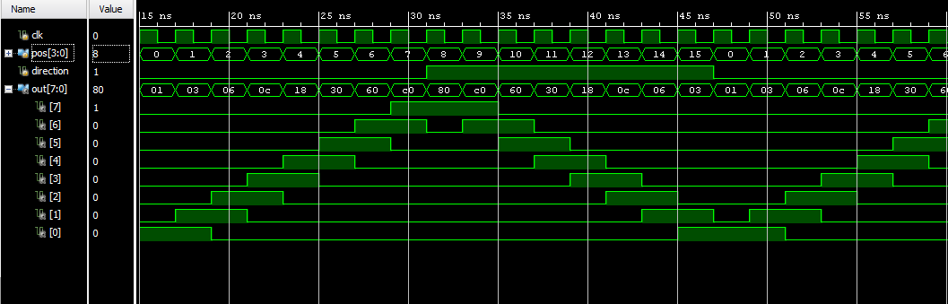
Fig. 1.12 Knight_rider’s simulation waveform
In Vivado, we can also debug our code by inserting breakpoints in Verilog’s code. This can be done by clicking on the empty circles that appear right of the line numbers in Vivado’s text editor. Other debugging functions such as Restart…, Run For…, Step, Break, etc. can be found in the toolbar or the Run menu. For more information on simulation and debugging see Xilinx's logic simulation tutorial.
After inspecting the simulated waveform, we can happily conclude that the knight_rider module performs as expected. We are ready to incorporate it into the block design.
1.4.2.3.4. Block Design
Any module in Vivado’s source folder can be added to the block diagram by right-clicking on the block design’s white canvas and choosing Add Module… Click on the knight_rider module and confirm. A new block with an RTL icon appears in the block diagram. To incorporate it into the structure, we connect the clk port to the output of the xlslice_0 block and the led_out port to the led_o external port as shown in the figure below. Note that starting with Vivado version 2020.1 and above, util_ds_buf_1 and util_ds_buf_2 have to be connected for a successful implementation.
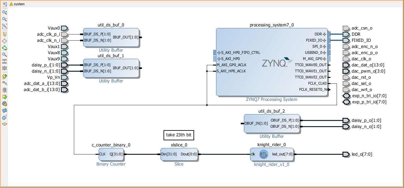
Fig. 1.13 Block Design
We can set the constant parameters of the module by double-clicking on the knight_rider_0 block and setting the two parameters as shown below.
LEDS_INIT = "1100000000"
DIR_INIT = 1
The Knight Rider module uses all 8 available LEDs on the Red Pitaya board. To connect the module’s output to all of them, we need to change the width of the external led_o port from 1 to 8 bits. This can be done by setting the led_o port’s LEFT parameter to 7 under the port properties (select the led_o port on the block design and locate the properties dialogue at the left-hand side of the IP Integrator). In the xlslice_0 block, set both the Din From and Din DownTo fields to 23.
The project is ready for synthesis, implementation, and generating bitstream. As we learned in the LED blink example copy the bitstream file to the Linux home folder on Red Pitaya and write it to the FPGA using the instructions below.
Please note that you need to change the forward slashes to backward slashes on Windows.
Open Terminal or CMD and go to the .bit file location.
cd <Path/to/RedPitaya/repository>/prj/Examples/Knight_rider/tmp/Knight_rider/Knight_rider.runs/impl_1
Send the .bit file to the Red Pitaya with the
scpcommand or use WinSCP or a similar tool to perform the operation.
scp system_wrapper.bit root@rp-xxxxxx.local:/root/Knight_rider.bit
Now establish an SSH communication with your Red Pitaya and check if you have the copy Knight_rider.bit in the root directory.
redpitaya> ls
Load the Knight_rider.bit to xdevcfg with
redpitaya> cat Knight_rider.bit > /dev/xdevcfg
The 2.00 OS uses a new mechanism of loading the FPGA. The process will depend on whether you are using Linux or Windows as the echo command functinality differs bewteen the two.
Please note that you need to change the forward slashes to backward slashes on Windows.
On Windows, open Vivado and use the TCL console. Alternatively, use Vivado HSL Command Prompt (use Windows search to find it). Navigate to the .bit file location.
On Linux, open the Terminal and go to the .bit file location.
cd <Path/to/RedPitaya/repository>/prj/Examples/Knight_rider/tmp/Knight_rider/Knight_rider.runs/impl_1
Create .bif file and use it to generate a binary bitstream file (system_wrapper.bit.bin)
Windows (Vivado TCL console or Vivado HSL Command Prompt):
echo all:{ system_wrapper.bit } >  system_wrapper.bif
bootgen -image system_wrapper.bif -arch zynq -process_bitstream bin -o system_wrapper.bit.bin -w
Linux and Windows (WSL + Normal CMD):
echo -n "all:{ system_wrapper.bit }" >  system_wrapper.bif
bootgen -image system_wrapper.bif -arch zynq -process_bitstream bin -o system_wrapper.bit.bin -w
Using a standard command prompt, send the .bit.bin file to the Red Pitaya with the
scpcommand or use WinSCP or a similar tool to perform the operation.scp system_wrapper.bit.bin root@rp-xxxxxx.local:/root/Knight_rider.bit.bin
Now establish an SSH communication with your Red Pitaya and check if you have the copy Knight_rider.bit.bin in the root directory (you can use Putty or WSL).
redpitaya> lsFinally, we are ready to program the FPGA with our own bitstream file located in the /root/ folder on Red Pitaya. To program the FPGA simply execute the following line in the Red Pitaya Linux terminal that will load the Knight_rider.bit.bin image into the FPGA:
redpitaya> fpgautil -b Knight_rider.bit.bin
The LEDs on your Red Pitaya should now blink in the famous Knight Rider fashion.
1.4.2.3.5. Double Knight Rider
We can make another Knight Rider light sequence where two sets of light streams move in opposite, mirrored directions. This can be done by adding another instance of the knight_rider module to the block design. The input clk of the new block is connected to the same clock as the first knight_rider module. The outputs of the two modules have to be first joined by a vector logic OR block, whose output is then wired to the led_o port. As we have learned in the LED blink example the vector logic block can be found under Xilinx’s IP cores (right-click on the white block design canvas and choose Add IP…). It will perform a pair-wise logic operation for each pair of elements in the two input vectors. To get the mirrored behavior of the second knight_rider block, its parameters should be set as:
LEDS_INIT = "0000000011"
DIR_INIT = 0
The block design for the Double Knight Rider is shown in the following figure.
Note
util_ds_buf_1 and util_ds_buf_2 must be connected for the implementation to be successful.
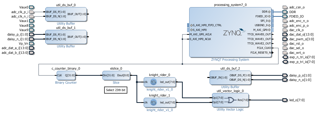
Fig. 1.14 Block Design
The Double Knight Rider light sequence is a great demonstration of the parallel nature of the FPGA. We simply added another instance of the module and connected it to the clock. Both blocks are implemented as separate logic circuits on the FPGA, running perfectly in parallel. The project is again ready for synthesis, implementation, and bitstream generation. Enjoy the light show on your Red Pitaya! You can of course change the frequency of the blinking LEDs by changing the parameter in the xlslice_0 block.
1.4.2.3.6. Automatic generation of the example from the repository
First, download the Red Pitaya FPGA Git repository to your computer and navigate to the RedPitaya-FPGA/prj/Examples folder.
Open the make_project.tcl file, uncomment the line “set project_name Knight_rider”, and comment all other “set project” lines.
Open Vivado 2020.1 and in Vivado Tcl Console navigate to the base folder: RedPitaya-FPGA/prj/Examples.
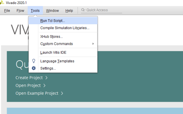
Then run the script by typing into the following command into the TCL console. If the TCL console is not open got to Tools → Run Tcl Script:
source make_project.tcl
make_project.tcl automatically generates a complete project in the RedPitaya-FPGA/prj/Examples/Knight_rider/ directory.
Take a moment to examine the block design.
If the Block Design is not open, click on Flow => Open Block Design from the top menu or select Open Block Design on the left-hand side of the window (under IP INTEGRATOR). When you are ready, click Generate Bitstream at the bottom-left part of the window to generate a bitstream file.
After you confirm that both Synthesis and Implementation will be executed beforehand, the longer process starts. After successful completion of synthesis, implementation, and bitstream generation, the bit file can be found at Examples/Knight_rider/tmp/Knight_rider/Knight_rider.runs/impl_1/system_wrapper.bit.
Finally, we are ready to program the FPGA with our own bitstream file.
1.4.2.3.7. Conclusion
Congratulations on creating the Knight Rider project!
In this project, we built a simple but nontrivial FPGA application – Knight Rider Lights – ideal for learning the basic concepts of FPGA programming. In this post, we got familiar with the Verilog language, which we used to create our module. We tested this module using Vivado’s simulator and finally inserted one or more instances into the block diagram. For the first time, we had to think in terms of circuits, where wires connect different parts of the system and where different blocks can run independently from each other. This inherent parallelism is one of the reasons why FPGAs are so popular for example in the high-performance computing. In the first two projects, FPGA programs were completely determined at the design level, without control during execution.
We will learn in the next project how to interface programmable logic with external signals, for example, ADCs, and how to write to and read data from registers on the FPGA using Linux running on the Zynq ARM processor.
If you want to roll back to the official Red Pitaya FPGA program, run the following command:
redpitaya> cat /opt/redpitaya/fpga/fpga_0.94.bit > /dev/xdevcfg
redpitaya> overlay.sh v0.94
or simply restart your Red Pitaya.