1.4.2.5. Frequency Counter
1.4.2.5.1. Introduction
On the way to a powerful acquisition system, let us make a quick detour and create a useful and simple project – a frequency counter. Yes, to measure frequencies, one can use Red Pitaya’s native apps such as Oscilloscope or Spectrum Analyzer. However, our program will be able to determine frequencies with much higher resolution, and at the same time, we will learn how to use Red Pitaya’s 125 Msps 14-bit ADC and DAC peripherals in the FPGA program.
This project contains two separate parts: the data acquisition part with a frequency counter and LED data display, and the signal generator part. To communicate with these two parts, we use the General Purpose IO block for setting configuration values and reading the counter output.
The frequency counter will be implemented in the reciprocal counting scheme, where a period of time of a predefined number of signal oscillations is measured and then inverted and divided by the number of oscillations. Such a scheme can yield a much better frequency resolution, especially for low frequency signals, compared to the conventional method where the number of signal cycles is counted at a predefined gate time.
1.4.2.5.2. Generation of an example from the repository
1.4.2.5.2.1. IP Cores
Some ip cores are required for block design. To create them, open the vivado tcl console and navigate to the RedPitaya-FPGA/prj/Examples/Frequency_counter lesson folder, then run the make_cores.tcl script
cd C:/Projects/RedPitaya-FPGA/prj/Examples/Frequency_counter
source make_cores.tcl
As a result, you will have a set of required ip cores in the tmp/cores folder that you can add to your project.
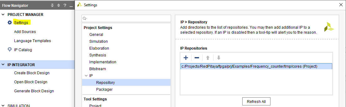
Fig. 1.16 Add Cores
1.4.2.5.2.2. Building the project
First, download the Red Pitaya FPGA Git repository to your computer and navigate to the RedPitaya-FPGA/prj/Examples folder.
Open the make_project.tcl file, uncomment the line “set project_name Frequency_counter”, and comment all other “set project” lines.
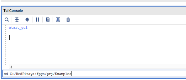
Open Vivado 2020.1 and in Vivado Tcl Console navigate to the base folder: RedPitaya-FPGA/prj/Examples.
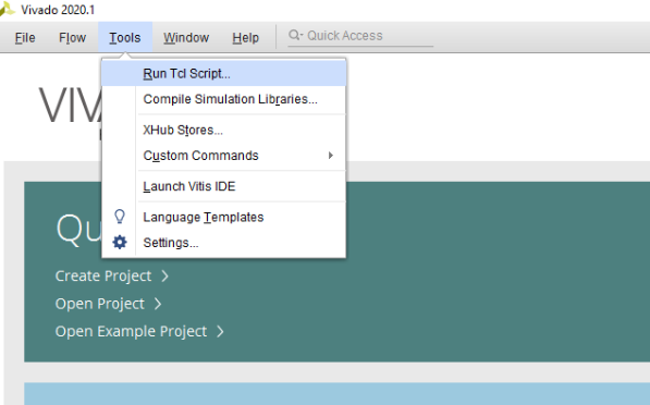
Then run the script by typing into the following command into the TCL console. If the TCL console is not open got to Tools → Run Tcl Script:
source make_project.tcl
make_project.tcl automatically generates a complete project in the RedPitaya-FPGA/prj/Examples/Frequency_counter/ directory.
Take a moment to examine the block design.
If the Block Design is not open, click on Flow => Open Block Design from the top menu or select Open Block Design on the left-hand side of the window (under IP INTEGRATOR). When you are ready, click Generate Bitstream at the bottom-left part of the window to generate a bitstream file.
After you confirm that both Synthesis and Implementation will be executed beforehand, the longer process starts. After successful completion of synthesis, implementation, and bitstream generation, the bit file can be found at Examples/Frequency_counter/tmp/Frequency_counter/Frequency_counter.runs/impl_1/system_wrapper.bit.
Finally, we are ready to program the FPGA with our own bitstream file.
Please note that you need to change the forward slashes to backward slashes on Windows.
Open Terminal or CMD and go to the .bit file location.
cd <Path/to/RedPitaya/repository>/prj/Examples/Frequency_counter/tmp/Frequency_counter/Frequency_counter.runs/impl_1
Send the .bit file to the Red Pitaya with the
scpcommand or use WinSCP or a similar tool to perform the operation.
scp system_wrapper.bit root@rp-xxxxxx.local:/root/Frequency_counter.bit
Now establish an SSH communication with your Red Pitaya and check if you have the copy Frequency_counter.bit in the root directory.
redpitaya> ls
Load the Frequency_counter.bit to xdevcfg with
redpitaya> cat Frequency_counter.bit > /dev/xdevcfg
The 2.00 OS uses a new mechanism of loading the FPGA. The process will depend on whether you are using Linux or Windows as the echo command functinality differs bewteen the two.
Please note that you need to change the forward slashes to backward slashes on Windows.
On Windows, open Vivado and use the TCL console. Alternatively, use Vivado HSL Command Prompt (use Windows search to find it). Navigate to the .bit file location.
On Linux, open the Terminal and go to the .bit file location.
cd <Path/to/RedPitaya/repository>/prj/Examples/Frequency_counter/tmp/Frequency_counter/Frequency_counter.runs/impl_1
Create .bif file and use it to generate a binary bitstream file (system_wrapper.bit.bin)
Windows (Vivado TCL console or Vivado HSL Command Prompt):
echo all:{ system_wrapper.bit } >  system_wrapper.bif
bootgen -image system_wrapper.bif -arch zynq -process_bitstream bin -o system_wrapper.bit.bin -w
Linux and Windows (WSL + Normal CMD):
echo -n "all:{ system_wrapper.bit }" >  system_wrapper.bif
bootgen -image system_wrapper.bif -arch zynq -process_bitstream bin -o system_wrapper.bit.bin -w
Using a standard command prompt, send the .bit.bin file to the Red Pitaya with the
scpcommand or use WinSCP or a similar tool to perform the operation.scp system_wrapper.bit.bin root@rp-xxxxxx.local:/root/Frequency_counter.bit.bin
Now establish an SSH communication with your Red Pitaya and check if you have the copy Frequency_counter.bit.bin in the root directory (you can use Putty or WSL).
redpitaya> lsFinally, we are ready to program the FPGA with our own bitstream file located in the /root/ folder on Red Pitaya. To program the FPGA simply execute the following line in the Red Pitaya Linux terminal that will load the Frequency_counter.bit.bin image into the FPGA:
redpitaya> fpgautil -b Frequency_counter.bit.bin
1.4.2.5.3. Project overview
The full block design of the frequency counter project is composed of six parts:
Processing System
GPIO
Signal Generator
Data Acquisition
Frequency Counter and Signal Decoder blocks, as shown in the figure below
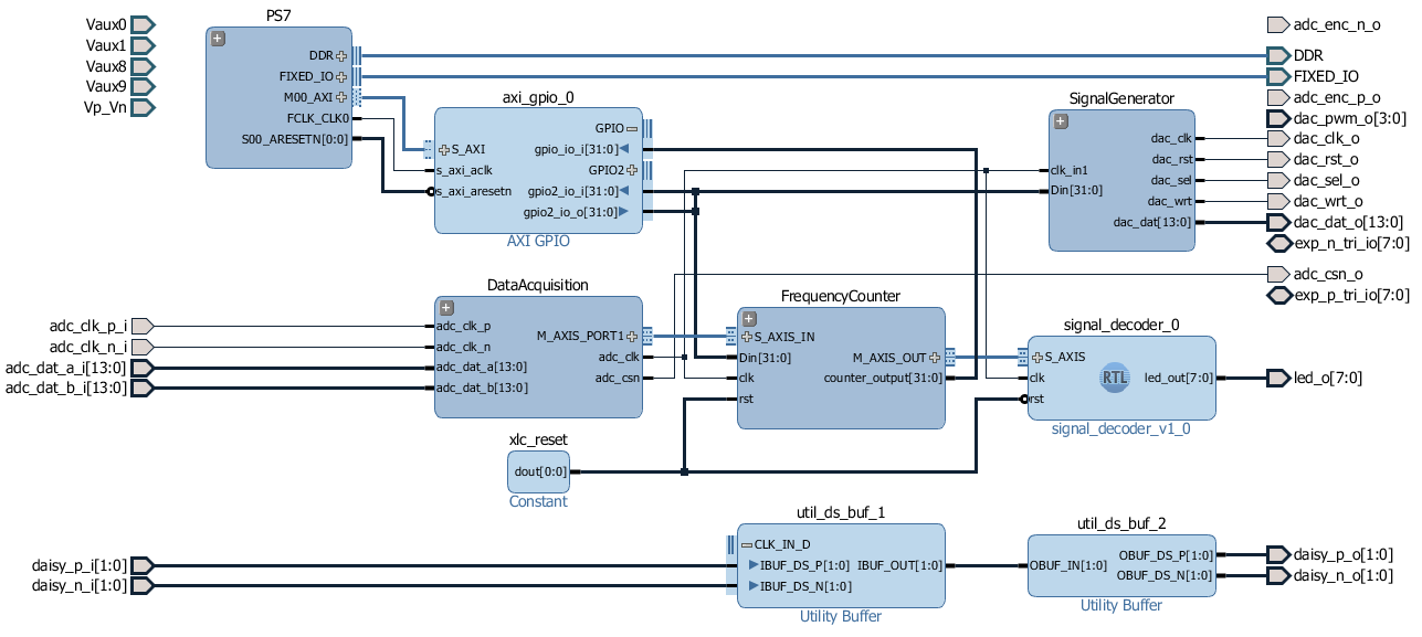
Fig. 1.17 Block Design Overview
These parts will be described in detail below. You can skip the lengthy description and go directly to the fun part at the end of the post.
1.4.2.5.4. Processing system
Let’s start with the most common part—the processing system IP core. Together with the AXI Interconnect and Processor System Reset blocks, these are the most common blocks in most of the Zynq 7000 FPGA applications. Since they take quite some space and have a lot of connections, we will join them in a single hierarchy block, so they will take less space and make block design more transparent. To create a hierarchy, select the desired blocks, right click, and select Create Hierarchy. From now on, we will put into hierarchies most of the blocks with related functionality.
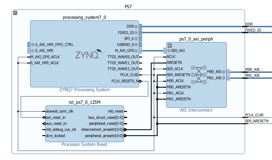
Fig. 1.18 Processing System 7 Hierarchy
1.4.2.5.5. General Purpose Input-Output Core
In the previous lesson, we learned how to write and read FPGA logic. We will use the same approach here for setting configurations such as the number of cycles and the signal generator’s phase increment. We will use the first GPIO port as an input to make the results of the frequency counter available to a program running on the Linux side. The second GPIO port will be used as a 32-bit output port, containing a 27-bit phase_inc value for the signal generator and a 5-bit log2Ncycles value for the frequency counter:
If you ever need more configuration output bits, you can use Pavel Demin’s axi_configuration IP core with a custom number of bits in a single output port. As described above, the axi_configuration file can be found in the Frequency_counter/core folder, which is automatically created with the make_cores.tcl script.
1.4.2.5.6. Signal Generator
The Signal Generator hierarchy generates sin (ωt) and cos(ωt) signals with a user-defined frequency at the two DAC output ports. The analog signal is generated by three blocks: the DDS compiler for calculating 14-bit sinusoidal values; the Clock Wizard to create a double clock frequency which allows setting the two DAC channels on each input clock cycle; and the AXI-4 Stream Red Pitaya DAC core for setting signal values to the external DAC unit. We will use 125 MHz adc_clock as the input clock to achieve a 125 Msps data rate.
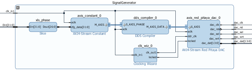
Fig. 1.19 Signal Generator Hierarchy
Frequency, amplitude, and other parameters can be set in the Direct Digital Synthesizer (DDS) re-customization dialog. The current DDS core settings will generate sin (ωt) on one DAC channel and cos(ωt) on the other, with a maximum amplitude of +/-1V (maximal range) on both.
The synthesised signal frequency is in the DDS compiler, determined by a phase increment value at each clock cycle. A nice description of the signal synthesiser operation can be found in the DDS compiler product guide. The signal frequency can be set fixed at the design stage by choosing Fixed Phase Increment in the DDS re-customization dialog. In this case, the dialog automatically calculates the required constant phase increment for a desired frequency and frequency resolution. Note that the output frequency will be a divisor of the clock frequency and might therefore deviate from the requested frequency.
Since we want to change the frequency during an operation, we choose Streaming Phase Increment in the re-customization dialog, which requires a phase increment value to be continuously supplied to the S_AXIS_PHASE input interface. The AXIS interface implements the AXI4-Stream protocol developed for fast directed data flow. It implements the basic handshake by utilising at least the tvalid and tready signals, but we will ignore even those for our nearly constant phase increment value. To create a continuous stream of the user-defined values, we use Pavel Demin’s AXI4-Stream Constant IP core, which converts the 32-bit input bus to the AXIS master interface.
AXI4-Stream Constant:
`timescale 1 ns / 1 ps

module axis_constant #
(
    parameter integer AXIS_TDATA_WIDTH = 32
)
(
    // System signals
    input  wire                        aclk,

    input  wire [AXIS_TDATA_WIDTH-1:0] cfg_data,

    // Master side
    output wire [AXIS_TDATA_WIDTH-1:0] m_axis_tdata,
    output wire                        m_axis_tvalid
);

    assign m_axis_tdata = cfg_data;
    assign m_axis_tvalid = 1'b1;

endmodule
Using the Slice IP core, we take a 27-bit phase_inc value from the gpio2_io_o port as input. Calculation of the phase_inc for a desired output frequency will be discussed in the last part of the post.
1.4.2.5.7. Data Acquisition
1.4.2.5.7.1. AXI4-Stream Red Pitaya ADC Core
The first block in the Data Acquisition hierarchy is the axis_red_pitaya_adc_v1_0 IP core, with two main features. First, it converts the external 125 MHz clock from adc_clk_a and adc_clk_b differential external ports into our programmable logic as an adc_clk clock. Second, it reads the ADC data from two input channels, which becomes available on each adc_clk clock cycle and makes it available over the AXI Stream (AXIS) interface M_AXIS. The IP core axis_red_pitaya_adc_v1_0 makes use of two AXIS interface ports: the axis_tvalid port, which is always asserted, and the axis_tdata port, a 32-bit data port with new measurements available on every clock cycle. A 16-bit channel 2 value and a 16-bit channel 1 value are stored in the 32-bit axis_tdata.
Since Red Pitaya has a 14-bit ADC, the 16-bit value has its two most significant bits set to either 00 or 11, depending on the sign of the measured value. It is instructive to have a look at the Verilog code of the AXI4-Stream Red Pitaya ADC core.
`timescale 1 ns / 1 ps

module axis_red_pitaya_adc #
(
    parameter integer ADC_DATA_WIDTH = 14,
    parameter integer AXIS_TDATA_WIDTH = 32
)
(
    // System signals
    output wire                        adc_clk,

    // ADC signals
    output wire                        adc_csn,
    input  wire                        adc_clk_p,
    input  wire                        adc_clk_n,
    input  wire [ADC_DATA_WIDTH-1:0]   adc_dat_a,
    input  wire [ADC_DATA_WIDTH-1:0]   adc_dat_b,

    // Master side
    output wire                        m_axis_tvalid,
    output wire [AXIS_TDATA_WIDTH-1:0] m_axis_tdata
);
    localparam PADDING_WIDTH = AXIS_TDATA_WIDTH/2 - ADC_DATA_WIDTH;

    reg  [ADC_DATA_WIDTH-1:0] int_dat_a_reg;
    reg  [ADC_DATA_WIDTH-1:0] int_dat_b_reg;
    wire                      int_clk0;
    wire                                      int_clk;

    IBUFGDS adc_clk_inst0 (.I(adc_clk_p), .IB(adc_clk_n), .O(int_clk0));
    BUFG adc_clk_inst (.I(int_clk0), .O(int_clk));

    always @(posedge int_clk)
    begin
        int_dat_a_reg <= adc_dat_a;
        int_dat_b_reg <= adc_dat_b;
    end

    assign adc_clk = int_clk;

    assign adc_csn = 1'b1;

    assign m_axis_tvalid = 1'b1;

    assign m_axis_tdata = {
        {(PADDING_WIDTH+1){int_dat_b_reg[ADC_DATA_WIDTH-1]}}, ~int_dat_b_reg[ADC_DATA_WIDTH-2:0],
        {(PADDING_WIDTH+1){int_dat_a_reg[ADC_DATA_WIDTH-1]}}, ~int_dat_a_reg[ADC_DATA_WIDTH-2:0]};

endmodule
Note
Red Pitaya’s ADC core has an additional output port (adc_csn) connected to the external port adc_csn_o for clock duty cycle stabilization.
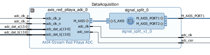
Fig. 1.20 Data Acquisition Hierarchy
1.4.2.5.7.2. Signal Split Module
The second block in the hierarchy is the signal_split RTL module. It transforms ADC output interface M_AXIS with two channel values into two M_AXIS output interfaces each containing a single channel value. The module has a very simple Verilog code, which can be found on Github.
`timescale 1ns / 1ps

module signal_split #
(
    parameter ADC_DATA_WIDTH = 16,
    parameter AXIS_TDATA_WIDTH = 32
)
(
    (* X_INTERFACE_PARAMETER = "FREQ_HZ 125000000" *)
    input [AXIS_TDATA_WIDTH-1:0]        S_AXIS_tdata,
    input                               S_AXIS_tvalid,
    (* X_INTERFACE_PARAMETER = "FREQ_HZ 125000000" *)
    output wire [AXIS_TDATA_WIDTH-1:0]  M_AXIS_PORT1_tdata,
    output wire                         M_AXIS_PORT1_tvalid,
    (* X_INTERFACE_PARAMETER = "FREQ_HZ 125000000" *)
    output wire [AXIS_TDATA_WIDTH-1:0]  M_AXIS_PORT2_tdata,
    output wire                         M_AXIS_PORT2_tvalid
);

    assign M_AXIS_PORT1_tdata = {{(AXIS_TDATA_WIDTH-ADC_DATA_WIDTH+1){S_AXIS_tdata[ADC_DATA_WIDTH-1]}},S_AXIS_tdata[ADC_DATA_WIDTH-1:0]};
    assign M_AXIS_PORT2_tdata = {{(AXIS_TDATA_WIDTH-ADC_DATA_WIDTH+1){S_AXIS_tdata[AXIS_TDATA_WIDTH-1]}},S_AXIS_tdata[AXIS_TDATA_WIDTH-1:ADC_DATA_WIDTH]};
    assign M_AXIS_PORT1_tvalid = S_AXIS_tvalid;
    assign M_AXIS_PORT2_tvalid = S_AXIS_tvalid;

endmodule
It is interesting to note that if you want to create an input or an output interface on an RTL module, simply name the input or output ports with a standard interface notation (see Vivado IP user guide). For example, in the signal_split RTL block, port names: S_AXIS_PORT1_tdata and S_AXIS_PORT1_tvalid are automatically combined into an S_AXIS_PORT1 interface.
1.4.2.5.8. Frequency Counter Module
The frequency counter hierarchy is based on the main RTL module frequency_counter, which has two main inputs: (1) the S_AXIS_IN* interface, which contains the measured single channel ADC signal, and (2) Ncycles, which specifies the number of signal oscillations for time measurement. Since the exact number of Ncycles is not important, the user specifies a 5-bit logarithmic value log2Ncycles via the GPIO core. Ncycles is then calculated as:
Using a pow2 RTL module. See the figure below.
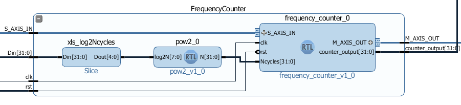
Fig. 1.21 Frequency Counter Hierarchy
The verilog code of the frequency_counter RTL module has three main parts. The first part directly wires the S_AXIS_IN to the M_AXIS_OUT interface so that data is transferred to the next block for processing. Instead, we could split the AXIS interface before the module. However, this would require an additional IP core – the AXI3-Stream Broadcaster.
`timescale 1ns / 1ps

module frequency_counter #
(
    parameter ADC_WIDTH = 14,
    parameter AXIS_TDATA_WIDTH = 32,
    parameter COUNT_WIDTH = 32,
    parameter HIGH_THRESHOLD = -100,
    parameter LOW_THRESHOLD = -150
)
(
    (* X_INTERFACE_PARAMETER = "FREQ_HZ 125000000" *)
    input [AXIS_TDATA_WIDTH-1:0]   S_AXIS_IN_tdata,
    input                          S_AXIS_IN_tvalid,
    input                          clk,
    input                          rst,
    input [COUNT_WIDTH-1:0]        Ncycles,
    output [AXIS_TDATA_WIDTH-1:0]  M_AXIS_OUT_tdata,
    output                         M_AXIS_OUT_tvalid,
    output [COUNT_WIDTH-1:0]       counter_output
);

    wire signed [ADC_WIDTH-1:0]    data;
    reg                            state, state_next;
    reg [COUNT_WIDTH-1:0]          counter=0, counter_next=0;
    reg [COUNT_WIDTH-1:0]          counter_output=0, counter_output_next=0;
    reg [COUNT_WIDTH-1:0]          cycle=0, cycle_next=0;


    // Wire AXIS IN to AXIS OUT
    assign  M_AXIS_OUT_tdata[ADC_WIDTH-1:0] = S_AXIS_IN_tdata[ADC_WIDTH-1:0];
    assign  M_AXIS_OUT_tvalid = S_AXIS_IN_tvalid;

    // Extract only the 14-bits of ADC data
    assign  data = S_AXIS_IN_tdata[ADC_WIDTH-1:0];


    // Handling of the state buffer for finding signal transition at the threshold
    always @(posedge clk)
    begin
        if (~rst)
            state <= 1'b0;
        else
            state <= state_next;
    end


    always @*            // logic for state buffer
    begin
        if (data > HIGH_THRESHOLD)
            state_next = 1;
        else if (data < LOW_THRESHOLD)
            state_next = 0;
        else
            state_next = state;
    end


    // Handling of counter, counter_output and cycle buffer
    always @(posedge clk)
    begin
        if (~rst)
        begin
            counter <= 0;
            counter_output <= 0;
            cycle <= 0;
        end
        else
        begin
            counter <= counter_next;
            counter_output <= counter_output_next;
            cycle <= cycle_next;
        end
    end


    always @* // logic for counter, counter_output, and cycle buffer
    begin
        counter_next = counter + 1; // increment on each clock cycle
        counter_output_next = counter_output;
        cycle_next = cycle;

        if (state < state_next) // high to low signal transition
        begin
            cycle_next = cycle + 1; // increment on each signal transition
            if (cycle >= Ncycles-1)
            begin
                counter_next = 0;
                counter_output_next = counter;
                cycle_next = 0;
            end
        end
    end

endmodule
The second part of the code sets the state buffer depending on the measured signal value relative to the high or low threshold values. If the signal is above the high threshold value, the state buffer is set to one, and if the signal is below the low threshold value, the state buffer is set to 0. Using two threshold values helps to prevent false state transitions in the case of noisy data.
The third section of code increments the counts register with each clock cycle, increments the cycles register with each positive state transition, and clears the cycles and counter registers when the number of cycles exceeds Ncycles. Before clearing the counter, its value is copied to the counter_output register, which is wired to the output port. The result of the frequency counter module is therefore a number of clock cycles in a time period of Ncycles signal oscillations, updated on each of the Ncycles signal oscillations. The frequency is then calculated as
1.4.2.5.9. Signal Decode Module
The final block in the ADC signal chain and in the block design is the signal_decode RTL module. Its purpose is to display the ADC value on the Red Pitaya LED bar, mostly for visual effects. The implementation is a simple 8-bit decoder from Vivado’s Language Templates. In the signal_decoder.v the three MSBs of the ADC value are decoded and displayed on LEDs.
`timescale 1ns / 1ps

module signal_decoder #
(
    parameter ADC_WIDTH = 14,
    parameter AXIS_TDATA_WIDTH = 32,
    parameter BIT_OFFSET = 4 // 4 for +/-20 V or 0 for +/-1 V ADC voltage range setting
)
(
    (* X_INTERFACE_PARAMETER = "FREQ_HZ 125000000" *)
    input [AXIS_TDATA_WIDTH-1:0]    S_AXIS_tdata,
    input                           S_AXIS_tvalid,
    input                           clk,
    input                           rst,
    output reg [7:0]                led_out
);
    wire [2:0] value;

    assign value = S_AXIS_tdata[ADC_WIDTH-BIT_OFFSET-1:ADC_WIDTH-BIT_OFFSET-3];

    always @(posedge clk)
        if (~rst)
            led_out <= 8'hFF;
        else
            case (value)
                3'b011  : led_out <= 8'b00000001;
                3'b010  : led_out <= 8'b00000010;
                3'b001  : led_out <= 8'b00000100;
                3'b000  : led_out <= 8'b00001000;
                3'b111  : led_out <= 8'b00010000;
                3'b110  : led_out <= 8'b00100000;
                3'b101  : led_out <= 8'b01000000;
                3'b100  : led_out <= 8'b10000000;
                default : led_out <= 8'b00000000;
            endcase
endmodule
However, if your ADC range jumpers are set to +/- 20 V instead of +/-1 V, you will see no activity when connecting the output of the Red Pitaya’s DAC to the input of its ADC port. In this case, the BIT_OFFSET parameter can be set to 4 to decode the 4th, 5th, and 6th signal’s MSBs. Shifting the bit position is related to signal amplification by a factor of 2. You can play with this value if the range is not optimal.
1.4.2.5.10. Pin assignment
Use the files in /prj/Examples/Frequency_counter/cfg for configuring the pins.
1.4.2.5.11. Fun Part
We are ready to test the frequency counter. Connect the Red Pitaya’s OUT1 port to the IN1 port. Save the project, create a bitstream and write it to the FPGA as described in the first chapter.
To run and control the frequency counter, you can use either the C or Python code below.
Keep in mind that the frequency resolution depends on the number of clock counts within the Ncycles signal oscillations. Low frequency signals require small Ncycles and high frequency signals require large Ncycles. The maximal number of counts is 2^32. The highest DAC frequency can be 125 MHz/4 = 31.25 MHz and the lowest frequency can be approx. 1 Hz. The conversion from the desired frequency into the phase_inc is done in the counter.c.
When setting the frequency to 2 Hz, the LED bar on the Red Pitaya board looks very much like Knight Rider’s lights (jumpers in the HV position). To make the code work for the LV position, change the BIT_OFFSET parameter in the signal_decoder.v.
1.4.2.5.11.1. C Program
Copy the program below ( counter.c is also in the Frequency_counter/server folder) to Red Pitaya’s Linux, compile it, and execute it as shown in the figure below.
#include <stdio.h>
#include <stdint.h>
#include <unistd.h>
#include <sys/mman.h>
#include <fcntl.h>
#include <stdlib.h>

int main(int argc, char **argv)
{
    int fd;
    int log2_Ncycles;
    uint32_t phase_inc;
    double phase_in, freq_in;
    uint32_t count;
    void *cfg;
    char *name = "/dev/mem";
    const int freq = 125000000; // Hz
    int Ncycles;

    if (argc == 3)
    {
        log2_Ncycles = atoi(argv[1]);
        freq_in = atof(argv[2]);
    }
    else
    {
        log2_Ncycles = 1;
        freq_in = 1.;
    }
    phase_inc = (uint32_t)(2.147482*freq_in);
    Ncycles = 1<<log2_Ncycles;

    if((fd = open(name, O_RDWR)) < 0)
    {
        perror("open");
        return 1;
    }

    cfg = mmap(NULL, sysconf(_SC_PAGESIZE), PROT_READ|PROT_WRITE, MAP_SHARED, fd, 0x42000000);


    *((uint32_t *)(cfg + 8)) = (0x1f & log2_Ncycles) + (phase_inc << 5);   // set log2_Ncycles and phase_inc

    count = *((uint32_t *)(cfg + 0));
    printf("Counts: %5d, cycles: %5d, frequency: %6.5f Hz\n", count, Ncycles, (double)freq/(count/Ncycles));


    munmap(cfg, sysconf(_SC_PAGESIZE));

    return 0;
}
Compile this code:
gcc counter.c -o counter.out
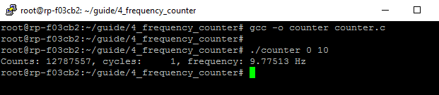
Fig. 1.22 Demonstration of counter.c program
The program can be used with the following parameters:
./counter {log2Ncycles} {frequency_Hz}
1.4.2.5.11.2. Python Program
You can also control the frequency counter with Python code through the Jupyter Notebook. After you have written the FPGA, connect to your Red Pitaya through the browser and navigate to the Jupyter Notebook application, which can be found in Development.
Open the Jupyter Notebook application, create a new notebook, copy the code below, save it, and finally execute it.
import mmap
import os
import time
import numpy as np

# OS 1.04 or older
os.system('cat /root/Frequency_counter.bit > /dev/xdevcfg')
# OS 2.00 and above
# os.system('fpgautil -b /root/Frequency_counter.bit.bin')

axi_gpio_regset = np.dtype([
    ('gpio1_data'   , 'uint32'),
    ('gpio1_control', 'uint32'),
    ('gpio2_data'   , 'uint32'),
    ('gpio2_control', 'uint32')
])

memory_file_handle = os.open('/dev/mem', os.O_RDWR)
axi_mmap = mmap.mmap(fileno=memory_file_handle, length=mmap.PAGESIZE, offset=0x42000000)
axi_numpy_array = np.recarray(1, axi_gpio_regset, buf=axi_mmap)
axi_array_contents = axi_numpy_array[0]

freq = 125000000 #FPGA Clock Frequency Hz
log2_Ncycles = 1
freq_in = 2
phase_inc = 2.147482*freq_in
Ncycles = 1<<log2_Ncycles

axi_array_contents.gpio2_data = (0x1f & log2_Ncycles) + (int(phase_inc) << 5)
time.sleep(1) #Allow the counter to stabilise

count = axi_array_contents.gpio1_data
print("Counts: ", count, " cycles: ",Ncycles, " frequency: ",freq/(count/Ncycles),"Hz\n")
1.4.2.5.12. Conclusion
Congratulations!!! You have successfully created the Frequency counter project!
If you want to roll back to the official Red Pitaya FPGA program, run the following command:
redpitaya> cat /opt/redpitaya/fpga/fpga_0.94.bit > /dev/xdevcfg
redpitaya> overlay.sh v0.94
or simply restart your Red Pitaya.